ATI Japan stands for
ADVANCED TECHNOLOGY INNOVATION JAPAN.
We are experts in semiconductor material processing, supporting the future of AI and optoelectronic fusion.
We are Semiconductor Material Processing Experts Supporting the Future of Optical Communication and Semiconductors.
ATI Japan Corp. contributes to the foundation of the global information society by processing and supplying high-quality semiconductor materials indispensable for the development of optical communication technology.
Our strength lies in high technical capabilities and flexible production support for products like
SOI (Silicon-on-Insulator) wafers and ultra-thick thermal oxide films,
which are required for cutting-edge fields such as photonics and PLC-AWG.
Through collaboration with domestic and international R&D institutions and cutting-edge equipment manufacturers, we continuously evolve as a partner supporting the next-generation optical communication infrastructure.
Connecting the world with light—at its core is the technology of ATI Japan.
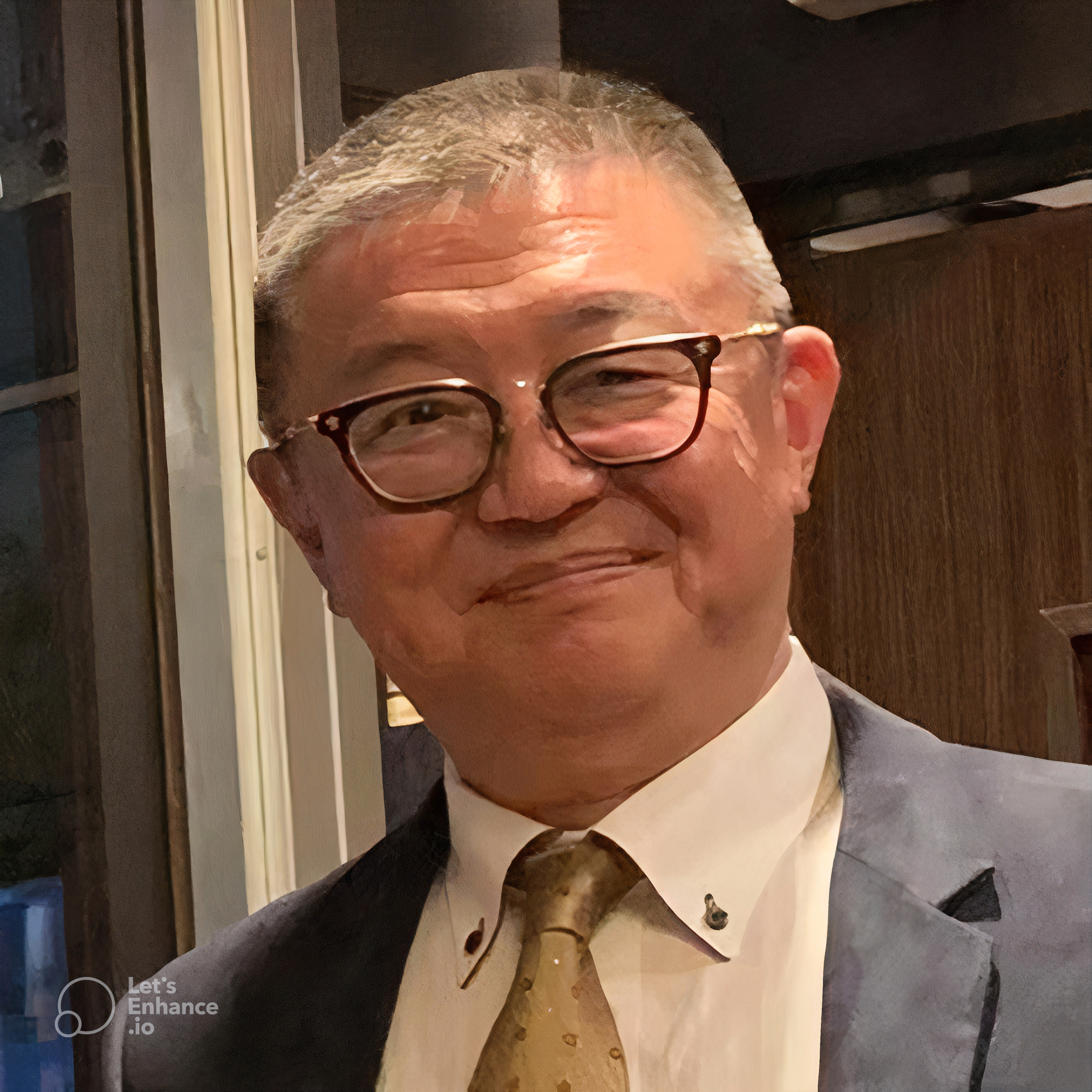
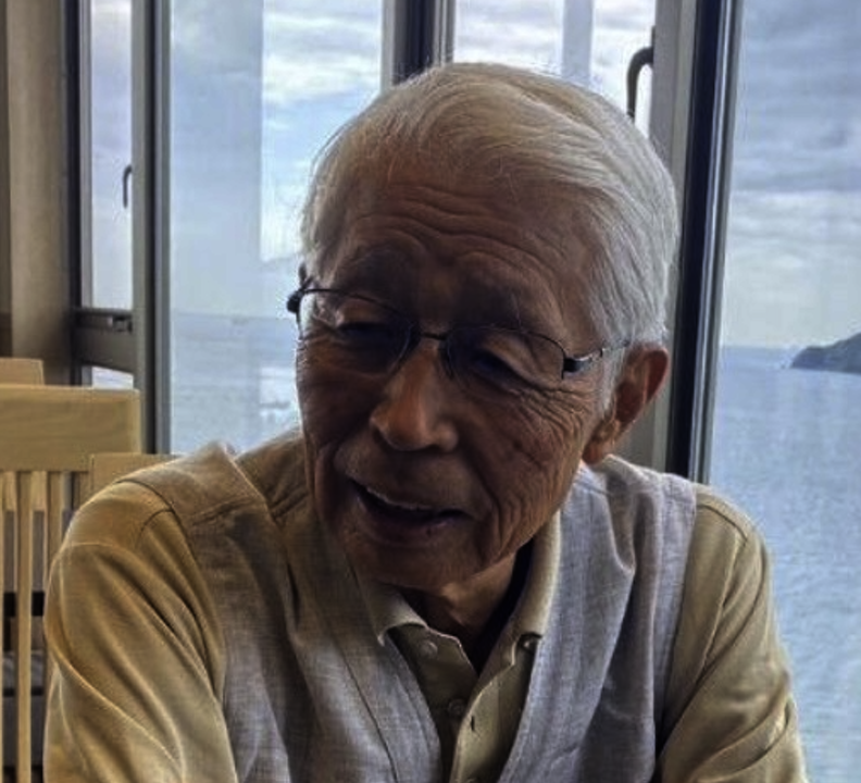
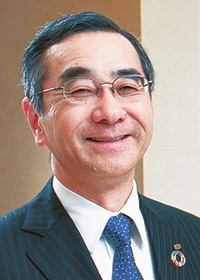
CEO Msg
ATI Japan Corp.
Representative Director Masahiro Kawasaki
ATI Japan Corp.,
centered on world-class ultra-thick thermal oxide film manufacturing technology, provides solutions that support the future of the optical communication and semiconductor industries.
Our proprietary ultra-thick thermal oxide film manufacturing technology achieves unparalleled thickness and high quality, earning high praise from domestic and international customers.
Currently, the optical communication and semiconductor industries are becoming increasingly important as the core of next-generation industries such as data centers, AI, and electric vehicles.
Through the most advanced film deposition process, our company is committed to enhancing the performance and reliability of critical devices supporting these industries.
At the same time, we are expanding our view from Japan to the world, collaborating with international partners to deepen R&D and manufacturing technology.
We firmly believe in the maxims of "being sincere about technology," "seriously engaging with customers," and "pursuing ultimate quality," and we aim to be a company that continuously takes on challenges.
We kindly ask for your continued support and guidance to ATI Japan.
Biography of Representative Director Masahiro Kawasaki
Career of Masahiro Kawasaki, Representative Director
May 1998 Established KST World Co., Ltd. in Fukui City, Fukui Prefecture.
March 1999 Established Kawasaki Semiconductor Technology America Corp. (KST America).
Opened offices in California and Arizona. Served as CEO.
January 2013 Established Kawasaki Semiconductor Technology Taiwan Corp. (KST Taiwan).
Opened office in Kaohsiung City. Served as Chairman.
Kawasaki Semiconductor Technology Taiwan Corp.
January 2022 Stepped down as Representative Director and President of Seiren KST Co., Ltd.
March 2022 Established ATI Japan Corp.
Corporate Philosophy
■ Mission To change the world of optical communication and semiconductors with the world's highest-level ultra-thick thermal oxide film manufacturing technology.
ATI Japan contributes to the advancement and reliability improvement of the optical communication and semiconductor industries through its ultra-thick thermal oxide film manufacturing technology. We strive to realize a sustainable affluent society through creativity and realization capability.
■ Vision To become a globally recognized technical brand where "ATI Japan is synonymous with ultra-thick thermal oxide film."
Our goal is to continuously maintain world leadership in quality, performance, and technological innovation, and to be the company of choice for customers and the industry.
■ Values
The values we cherish: Sincerity and Trust
Always maintain a sincere attitude toward both technology and people. Challenge Technological Innovation
Not satisfied with the status quo, continuously challenge the limits of processes and equipment. Quality First Principle
Pursue uncompromising quality in a world demanding nano-level precision. Customer-Centric Manufacturing
Listen to customer voices and walk the path of solving challenges together. Global Perspective
Deliver technology originating in Japan to the world and create international value.
Quality Policy / Environmental Commitment
■ Quality Policy
ATI Japan Corp. shall always provide quality that meets customer expectations through the world's top ultra-thick thermal oxide film manufacturing technology.
We commit to quality improvement company-wide based on the following fundamental policies for quality activities: ・Uncompromising quality principle pursuing nano-level precision ・Continuous improvement starting from customer feedback ・Thorough standardization and visualization of processes, equipment, and materials ・Operation and continuous improvement of the Quality Management System (QMS) ・Providing trust through simultaneous pursuit of quality and safety
■ Environmental Commitment
ATI Japan Corp. recognizes global environmental protection as a vital corporate responsibility and promotes the development and operation of clean and sustainable film deposition technology.
We will implement the following environmental actions: ・Development and introduction of energy-saving and resource-conserving film deposition technology ・Thorough waste reduction, sorting, and recycling ・Compliance with environmental laws/regulations and transparent disclosure of information ・Raising environmental awareness among all employees and practicing action ・Promotion of corporate activities aimed at realizing a sustainable society
Company Overview
ATI Japan Corp.
• Company Name : ATI Japan Corp. (Japanese: ATI Japan 株式会社)
• Date of Establishment : March 18, 2022
• Representative Director : Masahiro Kawasaki
• Head Office Address : 3-16-14 Nishishinagawa, Shinagawa-ku, Tokyo
• Nihonbashi Office : JACC Building 4F, 2-8-5 Nihonbashi Horidome-cho, Chuo-ku, Tokyo
• Capital : 130.35 million JPY, Capital Reserve: 130.35 million JPY
• Main Banks : Mizuho Bank Shibuya Chuo Branch, MUFG Bank Nihonbashi Branch
• Secondhand Dealer License : Tokyo Metropolitan Public Safety Commission Permit No. 301042422058
• Invoice Number : T4010001225392
• Associations etc. : Japan-China Economic Association Supporting Member,
MEMS Park Consortium Member
• Business Partners :
Company History
History of ATI Japan Corp.
March 2022: Established in Chuo-ku, Tokyo
May 2023: Relocated to Shinagawa-ku, Tokyo
October 2024: Opened "Nihonbashi Office" in Nihonbashi Horidome-cho, Chuo-ku, Tokyo
March 2025: Established ATIJ Hong Kong Limited
Executives
Board Members
Representative Director (CEO): Masahiro Kawasaki
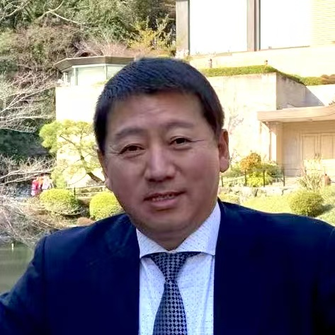
Director: Enyo O
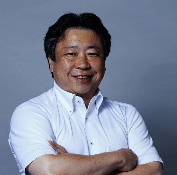
Director: Tetsuya Naito
Director: Masamitsu Yoshizawa
Auditor: Yoshikazu Kamiya
Representative Director (CEO)
Masahiro Kawasaki
Director
Enyo O
Director
Tetsuya Naito
Director
Masamitsu Yoshizawa
Advisors
Masayoshi Esashi
Masayoshi Esashi:CTO, MEMS Core Co., Ltd.
Concurrent Senior Research Fellow, Tohoku University
2022 - Order of the Sacred Treasure, Gold and Silver Star
Ryutaro Maeda
Ryutaro Maeda:National Institute of Advanced Industrial Science and Technology (AIST)
Emeritus Researcher, Device Technology Research Institute
Distinguished Professor, School of Instrument Science and Engineering, Xi'an Jiaotong University
Takunori Taira
Takunori Taira:Group Director, RIKEN SPring-8 Center
Specially Appointed Professor, Institute for Molecular Science, National Institutes of Natural Sciences
OPTICA (OSA), SPIE, IEEE Fellow
Fumiyuki Ota
Fumiyuki Ota:Former General Manager, Toshiba Oita Plant, Former Vice President, Dominion Semiconductor,
Former President, Tokuyama Toshiba Ceramics, Former Director, KST World
Actual Device Manufacturing (IC, Power Devices, MEMS, etc.)
Highest
・Surface roughness, defect density, particles are strictly controlled
・Most stable electrical properties and crystal defects
High
Monitor Grade
Process Monitoring in Mass Production Lines
High (Close to Prime)
・Supplied with the same crystal orientation, conductivity type, and resistivity as product wafers
・Defect tolerance is looser than Prime・Performance and quality are equivalent to Prime during the process
Medium (Cheaper than Prime)
Test Grade
Equipment Startup, Trial Processing, Research Applications
Medium
・Allows surface defects and micro-scratches・Electrical properties are not emphasized
・Reproducibility of product performance is not as strictly required as Monitor
Relatively Cheap
Dummy Grade
Handling Practice, Equipment Calibration, Physical Practice
Low
・Allowed to contain more cracks and defects
・Conductivity type, resistivity, etc., are usually not specified
・Essentially treated as a "silicon disc"
Cheapest
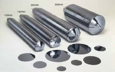
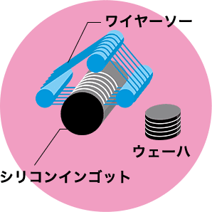
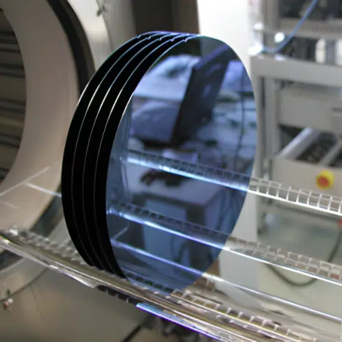
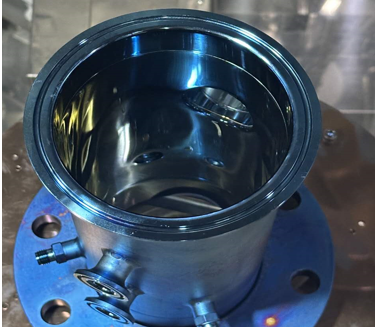
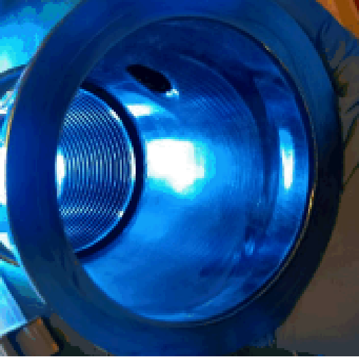
Ultra-Thick Film to Thin Film Thermal Oxide Wafers
ATI Japan uses the thermal oxidation method to deposit ultra-thick films. This achieves film quality unattainable with the CVD method.
Currently, we can handle film deposition in the range of 2µm to 20µm, which is considered difficult with the thermal oxidation method.
Wafer diameters supported are 6 inch (150mm), 8 inch (200mm), and 12 inch (300mm).
Thick films are widely used in optical communication, MEMS, medical, power devices, and other fields.
Thin films can be used for testing, evaluation, development, and other purposes.
InP (Indium Phosphide) Wafers・・・Official Japan Agent for Grenoble InPACT, France
Indium Phosphide manufacturer covering all dopants (Fe, Sn, Zn, S) and
all diameters (2", 3", 4")
Properties: High-efficiency semiconductor for high-frequency communication and optical communication. Applications: Lasers, optical amplifiers, optical fibers for optical communication, etc. Features: Possesses high electron mobility and high dielectric breakdown strength.
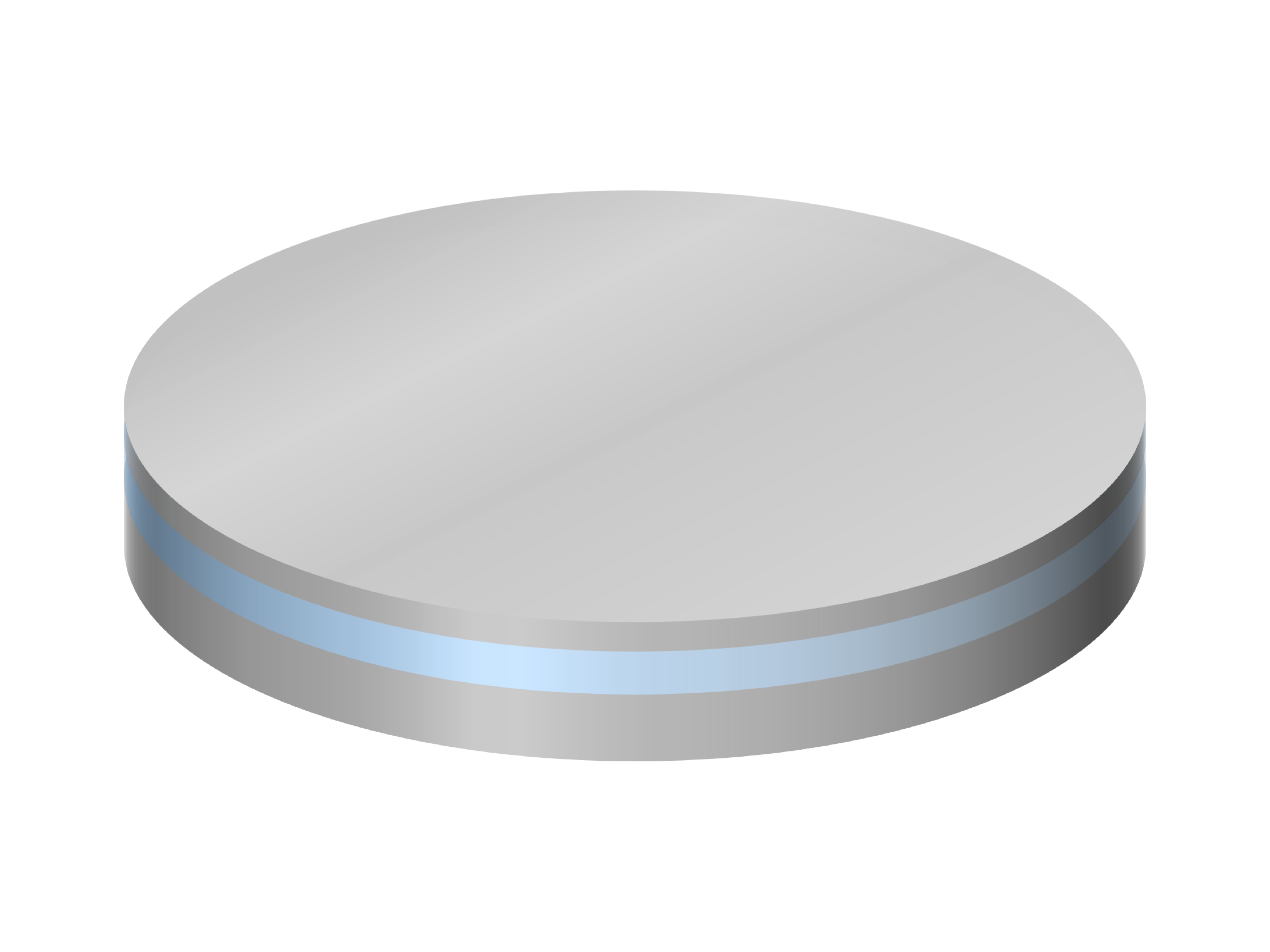
Thin Film SOI Wafers, Thick Film SOI Wafers, Bonded Wafers
・SOI (Silicon-on-Insulator)
ATI Japan offers SOI wafers of various specifications.
For small volumes and short lead times, you can choose from our stock SOI wafers.
Stock SOI wafers are available starting from one piece.
・Excellent Device Layer Uniformity (±0.1µm)
・Low Stress Close to Single Crystal Wafer
・Extremely Small Steps (0.5㎜)
・Extremely Thin Substrate Wafer (50µm~)
・POI Wafers, and other bonded wafers
・POI (Polymer-on-Insulator)
・SiC on Si
・GaN on Si
・Others
Please feel free to contact us regarding bonded wafers.
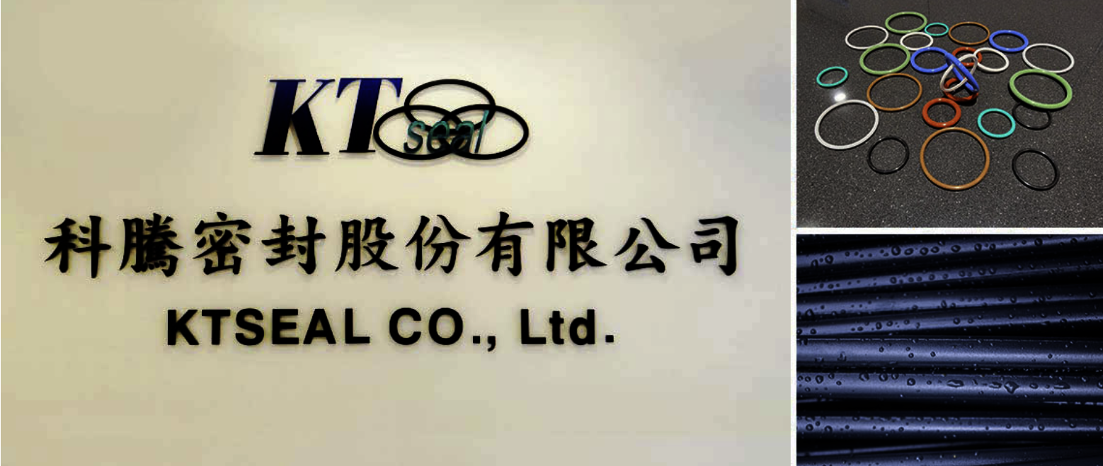
・O-ring
Official Japan agent for KT Seal, Taiwan, providing perfluoroelastomer O-rings with excellent chemical and plasma resistance.
Stable supply of O-rings officially adopted by TSMC and UMC.
We will be exhibiting at MEF2026 (MEMS Engineer Forum), held from Tuesday, April 21 to Wednesday, April 22, 2026.
The venue is KFC Hall in Ryogoku, Tokyo.
We will be showcasing our latest technologies and solutions at the event.
If you are attending, please be sure to stop by our booth.
Work
Adipiscing magna sed dolor elit. Praesent eleifend dignissim arcu, at eleifend sapien imperdiet ac.
Aliquam erat volutpat. Praesent urna nisi, fringila lorem et vehicula lacinia quam. Integer
sollicitudin mauris nec lorem luctus ultrices.
Nullam et orci eu lorem consequat tincidunt vivamus et sagittis libero. Mauris aliquet magna magna
sed nunc rhoncus pharetra. Pellentesque condimentum sem. In efficitur ligula tate urna. Maecenas
laoreet massa vel lacinia pellentesque lorem ipsum dolor. Nullam et orci eu lorem consequat
tincidunt. Vivamus et sagittis libero. Mauris aliquet magna magna sed nunc rhoncus amet feugiat
tempus.
About
Lorem ipsum dolor sit amet, consectetur et adipiscing elit. Praesent eleifend dignissim arcu, at
eleifend sapien imperdiet ac. Aliquam erat volutpat. Praesent urna nisi, fringila lorem et vehicula
la
lacinia quam. Integer sollicitudin mauris nec lorem luctus ultrices. Aliquam libero et malesuada
fames ac ante ipsum primis in faucibus. Cras viverra ligula sit amet ex mollis mattis lorem ipsum
dolor sit amet.